Research

The properties of materials play a major role in society. Magnetic materials are used in generators and hard disks. Superconductors are essential for MRI scanners. The electrical properties of semiconductors are at the heart of integrated circuit technologies.

In recent years, new materials with counterintuitive magnetic and electrical properties have been discovered. Examples include graphene in which electrons behave like light, van-der-Waals magnets that enable two-dimensional (2D) spin transport, and insulating oxides that yield a 2D electron gas when stacked. Understanding how spins and charges move in these ‘quantum materials’ is interesting in its own right, but may also enable new functionalities and minimized dissipation in future devices.

Our group studies charge- and spin-transport in materials that are both fundamentally intriguing and potentially useful for devices. We are particularly interested in the collective behaviour that arises from particle interactions. The vision is to realize a set of nanoscale imaging and electronic-transport tools that enable new ways to address this topic. Along these lines, we have developed an new technique for imaging collective spin excitations known as spin waves (more below).

A central role in our lab is played by nitrogen-vacancy (NV) centers in diamond, which we use as magnetic-field sensors. This involves photoluminescence microscopy with single-photon sensitivity, single-spin microwave control, electronic transport, and scanning-probe microscopy. With these techniques we pursue the vision described above, focusing on two main research directions:

  • Spin-wave transport in thin-film magnets (largest effort)
  • Imaging electrical currents in quantum materials (just taking off in the context of our NWO VIDI project)

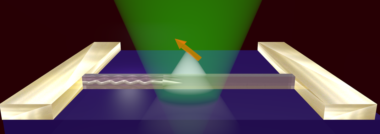
Spin waves Spin waves are the elementary excitations of magnetic materials. A growing research field is focusing on creating spin-wave technology, such as spin-wave transistors. Theory is addressing fundamental questions about nanoscale spin-wave transport, the interaction of spin waves with other excitations such as phonons, adding excitement by predicting exotic phenomena such as spin superfluidity and the spin-wave quantum-Hall effect. Being able to probe and control spin-wave transport with high resolution at buried magnetic interfaces is key to realizing these exciting prospects.

We have developed a new technique for imaging spin waves (Science Adv. 6, 3556 (2020)) using nitrogen-vacancy sensor spins in diamond. Because the imaging is magnetic - in key contrast with other spin-wave imaging techniques - we can ‘look through’ optically opaque materials . We are leveraging this capability to study the interaction between spin waves and metals. We recently demonstrated the dramatic impact of metals on the damping of spin waves (Adv. Quant. Tech. 2100094 (2021)) - important as the majority of applications and devices use metal electrodes to control spin waves. We study spin waves on the nanoscale using NV-diamond tips that we fabricate in our Kavli nanolab. This scanning-probe system enables few-nanometer proximity of the NV sensors to the material and, as a result, the detection of minute spin-wave stray fields with high spatial resolution. We use this system to study spin-wave interactions, and have discovered that spin waves generate high-density magnon gases (Nano Letters 21, 8213 (2021)). Such out-of-equilibrium magnon densities can be used to control spin currents and enable studying interactions within the magnon gas. By controlling the NV-magnet distance on the nanoscale, we selectively image the nanoscale spin waves generated via scattering (arXiv:2207.02798). We also develop electrical spectrocopy to study spin waves in magnetic insulators with small anisotropy (APL 119, 202403 (2021)) for realizing spin-wave optics.

… and more.